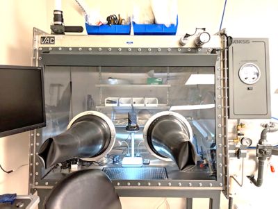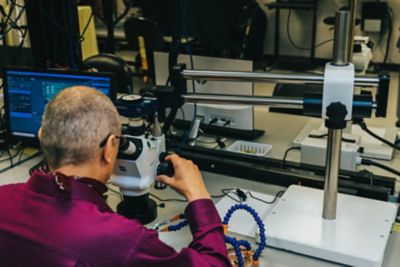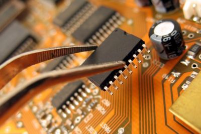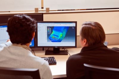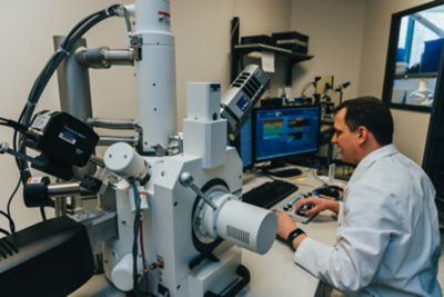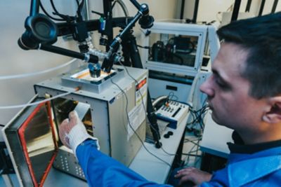

Featured Lab Capabilities
Ansys’ multi-million dollar test lab facility features 20,000 square feet of lab and test space, including 25 environmental chambers, component and sub-system testing and a full-service material characterization and failure analysis lab.
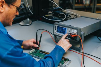
Our team of RES experts have decades of experience to get to the root of the problem, mitigate failure risks and devise practical solutions—all within your timeline and cost constraints.