

ANSYS BLOG
September 20, 2021
How to Identify Common Electronic Component Failures
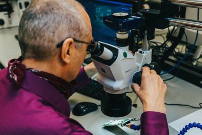
A member of the Ansys Reliability Engineering Services team looking for a failure mechanism under microscope.
Failure analysis is the process of identifying, and typically attempting to mitigate, the root cause of a failure. In the electronics industry, failure analysis involves isolating the failure to a location on a printed circuit board assembly (PCBA) before collecting more detailed data to investigate which component or board location is functioning improperly.
Electronics typically fail on a PCBA in one of three places:
- Within a component
- At the interconnect between a component and board (usually solder joints)
- Within the printed circuit board itself
Common Electronic Component-Level Failures
Component-level electronic failures refer to failures occurring within an electronic component that is soldered to a printed circuit board. Often, when a failure is isolated to a specific electronic component, further electrical characterization — such as comparative curve tracing — can be used to isolate the failure to a specific pin. This is crucial when the failure is located on a component with a large number of I/O pins. Some of the most common component level failures and failure analysis techniques that are used to identify them are discussed below.
Wire Bond Breaking and Liftoff
Wire bonds are small wires that connect an integrated circuit's die to its leads. They are thin and fragile, and can fracture under mechanical stress. The most common failure analysis technique used to identify wire bond breaking is X-ray microscopy. In most cases, X-ray images of an integrated circuit’s internal structure are enough to confirm or eliminate wire bond breaking as a failure mechanism. Acoustic microscopy can also gather data when wire bond fracture is a suspected failure mechanism. Because it can identify air gaps within a specimen, it can discover evidence of popcorn cracking, which can damage wire bonds.
A similar failure mechanism is wire bond liftoff, where the ball bond breaks at the intermetallic connection between the wire and the die, and lifts off the bond pad. This generally occurs due to issues during the bonding process. Several failure analysis options can identify and determine the root cause of wire bond liftoff. In severe cases, wire bond liftoff can be identified with X-ray microscopy; however, cross sectioning is typically required to confirm. Once bond liftoff is confirmed as the failure mechanism, further analysis can determine why the bond is lifting. The most common causes are chemical contamination on the bond pads or poorly formed, mashed balls due to incorrect pressure during the bonding process. Quality cross sections will enable the size and shape of the bond to be measured, along with the thickness of the intermetallic connection. In some cases, it may be necessary to pull or shear bonds off of the die to inspect the pad surface. Scanning electron microscopy (SEM) and energy dispersive X-ray spectroscopy (EDS) of a bond pad surface can reveal contamination that could create bonding issues.
Delamination
Delamination within a component typically refers to the separation of a molding compound from either the die or the lead frame of an integrated circuit. Delamination on the die surface creates the potential for moisture ingress that can lead to short circuits across the die. Acoustic microscopy is the non-destructive method most often used to identify delamination within a component. When the location of a suspected delamination is known, cross sectioning can also confirm it.
Capacitor Cracking
Multi-layer chip capacitors (MLCCs) can be prone to cracking under mechanical flexure or thermal shock. Flex cracking occurs when the board that the capacitor is soldered to experiences excessive bending, which can be caused during depaneling, connector insertion, fixturing, or other mechanical events. Thermal shock cracking occurs when the part experiences a sudden, dramatic temperature increase, such as from improper soldering. In either case, capacitor cracking can potentially cause component failures by increasing the risk of a short circuit within the capacitor body, either between the plates or between the plates and the terminals. 3D X-ray and acoustic microscopy can identify capacitor cracking; however, cross sectional analysis is often required to completely confirm. Cross sectioning and optical microscopy can also shed light on the root cause of the cracking. Flex cracks typically manifest as diagonal cracks between the horizontal and vertical regions of the component terminals while thermal shock cracks can occur in a variety of morphologies.
Die Damage
Die damage can manifest in a number of ways. Mechanical or thermo-mechanical overstress can physically crack the die, creating open circuits within the integrated circuit. This type of die cracking is typically egregious. It can be confirmed with acoustic microscopy, 3D X-ray microscopy, and, in some severe cases, 2D X-ray microscopy. Once the location of a die crack is known, cross sectional analysis can be used to examine the orientation and severity of the damage in more detail.
Diagram of a ball grid array (BGA). Engineers can use digital image correlation (DIC) to assess its thermal expansion or warpage due to thermo-mechanical loads.
Electrical overstress or electrostatic discharge also causes die damage of varying severity. Extreme electrical events can cause enough carbonization to be observable with X-ray microscopy; however, electrical die damage is often much more subtle. In these cases, more specialized die inspection techniques are necessary. A typical first step when electrical die damage of an integrated circuit is suspected is decapsulation of the component. Acid decapsulation can remove the overmold compound, exposing the die surface and the wire bonds, which enables optical inspection. If the damage is on the surface or in one of the upper layers of the active region, it can often be observed with optical microscopy or SEM after decapsulation. In cases of deeper or very subtle electrostatic overstress (EOS) or electrostatic discharge (ESD) damage, the die must be examined with a superconducting quantum interference device (SQUID), thermal imaging under electrical stress, or other specialized techniques to identify the exact failure location.
Interconnect-Level Failures
Interconnect-level failures are typically to broken solder joints or leads. Knowledge of an electronic assembly's environmental conditions can help to determine the likelihood of an interconnect level failure before beginning a failure analysis. The laboratory techniques used to identify the most common forms of component/board interconnect failure are discussed below.
Solder Fatigue
Solder fatigue occurs primarily due to temperature cycling over an extended time. The major driver of solder fatigue is the coefficient of thermal expansion mismatch between a PCB and a lead or component body. This effect can be accelerated by tensile stresses from potting or component warpage, excessive vibration, or increasing the size of the component. In many cases, optical inspection or X-ray microscopy can identify such failures; however, cross sectioning a joint is the most reliable method for confirming a fatigue failure. A quality cross section of solder joints can be examined for evidence of cracking or the grain growth/phase coarsening associated with continual stresses on solder. When cross sectioning is impractical, such as when the failing joint on a BGA with many pins is unknown, dye-and-pry techniques can identify solder joint cracking.
Classic solder fatigue illustration
Solder Overstress
Solder overstress occurs when a single mechanical event, such as a drop, results in a fractured solder joint. Optical microscopy and cross sectioning identifies over-stress fractures. Typically, cracked solder joints caused by mechanical overstress will have much larger gaps than those caused by solder fatigue.
Lead Fracture
Lead fracture is a failure mechanism that occurs when the solder joint of a component remains intact, but the metal lead itself breaks between the board and the body of a component. Lead fracture is most prevalent on large electrolytic capacitors and components with thin gull wing leads that experience excessive vibration and shock. Optical microscopy identifies lead fracture, and mechanical testing can be used to assess the risk of lead fracture in an electronic assembly.
Common Board-Level Electronic Failures
Board-level failures manifest on or within the printed circuit board itself. They can appear as short or open circuits and, depending on the complexity of the board's electrical networks and stack-up, can be much more difficult to locate than component- or interconnect-level failures.
Read the 6 Steps to Successful Board Level Reliability Testing whitepaper to learn more.
Contamination-Induced Current Leakage
Short circuits between component leads or exposed traces can occur on a board surface in humid environments when the board does not have adequate cleanliness. In severe cases, these shorts can be confirmed with optical microscopy or SEM/EDS. Ion contamination analysis can also be used as a board qualification technique to determine whether contamination levels on the board surface are below industry standard minimums.
Conductive Anodic Filament Failure
Conductive anodic filament (CAF) occurs when metal migrates along the fibers within the laminate layers of a PCB. CAF typically creates failures when it occurs between two closely spaced plated through holes (PTH). CAF failures are typically created as a result of excessive drill damage or poor glass/resin bonding and can be exacerbated by humid environments. Temperature/humidity bias testing can determine CAF risk of an electronic assembly prior to field use. When a CAF failure is expected, electrical testing is typically used to determine the affected via pair or pairs. Cross sectional analysis and optical microscopy must then confirm the presence of CAF and to determine the root cause of the metal migration. When the root cause is drill damage, large cracks will be noticeable around the edges of the through holes. In the case of poor glass/resin bonding, hollow tubes or voids can be observed within the glass weave in one or more of the laminate layers. SEM/EDS can also confirm the observed filament is metallic in nature.
Plated Through Hole Fatigue
PTH fatigue typically manifests in one of two forms: barrel cracking, when the plating on the through hole itself fractures; and trace cracking, when the connection between a PTH barrel and a normally attached trace breaks. PTH fatigue is most often a result of thermal cycling, as expansion of the laminate material in the out-of-plane direction transfers stresses to the PTH. 3D and, in severe cases, 2D X-ray microscopy can be used to identify PTH fractures; however, as PTH cracking is often very thin, cross sectional analysis and X-ray microscopy are typically used to confirm.
Pad Cratering and Trace Fracture
Pad cratering and trace fracture are failures that are associated with overstress events, like drop and other shocks. Pad cratering is a failure that occurs primarily under BGA solder joints. It occurs when mechanical stresses cause the pad to begin to rip off the board, creating a crater-shaped crack structure in the laminate layer underneath the ball pad. 3D X-ray, dye-and-pry analysis, cross sectional analysis, or, in very severe cases, simple optical inspection can be used to identify the presence of pad cratering under BGA pads.
Pad craters are often accompanied by trace fractures. Trace fractures occur when a thin trace breaks at the stress-concentrating interface between the routing and the ball pad. Trace fractures can also appear independent of pad cratering at other regions of the circuit board, typically at a stress concentration, like when a thin region of routing turns at an angle or connects to a large solder pad. Trace fractures can be very difficult to locate. Thorough knowledge of the electrical networks within the PCBA as well as a general idea of the mechanical loads applied to the PCBA are necessary to even formulate hypotheses about the location when a trace fracture is the suspected failure mechanism. X-ray microscopy can confirm the presence of a trace fracture in most cases, but it often a time-consuming activity as it can require a thorough scan of the network of interest at high magnification.
Electronic Product Design and Development Complications
Certain product design choices can make failure isolation extremely difficult. Potting, chassis, and fixturing can visually obscure and physically inhibit access to regions of the assembly, prohibiting electrical characterization or optical inspection. Assemblies with large amounts of metal can hamper the usefulness of X-rays by hiding the area of interest. Assemblies containing both very hard and very soft materials (for example, alumina and solder) can make quality cross sectioning difficult. In these and other unique cases, knowledge of the environment, PCBA properties, and electronic component types must be used to develop theories as to which components, solder joints, or board regions could be failing, and creative techniques may need to be employed to adequately confirm root cause of failure.
Ansys offers a multidisciplinary approach to our root cause analysis services that are effective in identifying how a problem originated, whether it occurred in the field, on a test or involved a loss of quality during manufacturing. Visit the Reliability Engineering Services page of our website to request a quote and learn more.
See What Ansys Can Do For You
See What Ansys Can Do For You
Contact Us
Contact us today