

Join Us for Simulation World 2024
The global simulation event designed to inspire, equip, and empower you to innovate.
May 14-16, 2024

Making Meaningful Connections Down the Road
See how Aptiv and Infineon are using digital engineering to sort through complexity and deliver the connected systems -- and systems of systems -- that make software-defined vehicles possible.

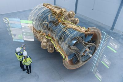
Unleash SimAI's Power in Engineering
Revolutionize Your Product Development with AI-Powered Simulations for Rapid Performance Prediction.

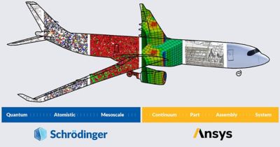
The Intersection of AI and Simulation Technology
Since the mid-20th century, scientists and engineers have tested, validated, and improved their designs with simulation. Simulation software generates synthetic data, and AI combines these learnings into real-time insights to fill in the gaps of what’s possible, making simulation faster.


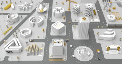
Solving the Unsolvable
Without simulation, there are no autonomous vehicles. No 5G networks. No space exploration. Ansys multiphysics software solutions and digital mission engineering help companies innovate and validate like never before.
The Latest From Ansys
See What Ansys Can Do For You
See What Ansys Can Do For You
Contact Us
Contact us today